This is an old revision of the document!
Table of Contents
SN74HC595(N) Shift Register
1. About the Module
As the monitoring station should be more or less self-sustainable later on, an important factor to consider is the power consumption of the devices. There are different sources of power losses that drain the batteries of the station over time. One such loss is the current that flows through the VDD pins to GND in the sensors while they are not used. This power loss could be lowered if the power supply would be just activated when the sensor is actually in use.
This could be done using a simple transistor. However, with a transistor, one GPIO pin of the MCU would be used for each device that is powered individually. When the number of sensors increase, the available GPIOs rapidly decrease. The same would be true for directly using GPIOs to power the sensors which should always be avoided; one reasons for that is, that the GPIOs can only supply a low current and do not have as stable voltage levels as the 3.3V pin.
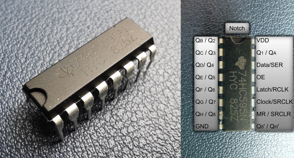
Another method is to use a shift register, such as the SN74HC595 (figure 1). That is a small integrated circuit (IC) which transforms a digital serial input into a digital parallel output. The SN74HC595 contains a shift register and a storage register of the size of 1 byte and possesses 8 parallel output pins. To operate the device 3 GPIO pins of the MCU are needed, one pin for transmitting the data (data, DS, SER), one pin for the clock signal of the shift register (clock, SHCP, SRCLK) and another one as clock signal for the storage register (latch, STCP, RCLK). The advantage of the shift register is that with only 3 GPIO pins, 8 output pins can be controlled at the same time individually. Furthermore, the IC has another output for serial data which can be connected to the serial input (data pin) of another shift register. This allows for the cascading, that means connecting many ICs in series, of the SN74HC595; so, with only 3 pins a large number of outputs can be managed.
Working Principle
The MCU issues a clock signal (SRCLK) to the shift register and sends the data (SER) bitwise in 8-bit groups to the shift register (figure 2). If afterwards another byte is sent, the shift register outputs the first byte through the serial output pin (QH’), which may be connected to another shift register receiving the data. So, the shift register always stores the latest byte and if it receives a new byte, it shifts the old one to the next shift register.
The byte stored in the shift register is transferred to the storage when a high voltage level signal is sent to the storage register through the storage register clock input (RCLK). The byte stored in the storage register defines which output pins should be active and which ones should be inactive. When the output enable pin (OE) is set to GND, the byte from the storage register is used as output on the output pins. When the output enable pin is high, the three-state outputs are in high impedance state, blocking all current through the output pins.
It can happen that the outputs from the shift register are random when for example uploading code or resetting the MCU. To reset the pins and stop any high output, the master reset pin (MR, SRCLR) must be shorted to ground. This can be done for example by connecting a >1 uF capacitor between GND and SRCLR and a 10kΩ resistor between SRCLR and VDD. After powering up, the capacitor acts as a short circuit to ground resetting the outputs and as soon as it is charged, it acts as an open circuit and the potential of the master reset is high.


